Description
Experience the RAMANdrive workflow.
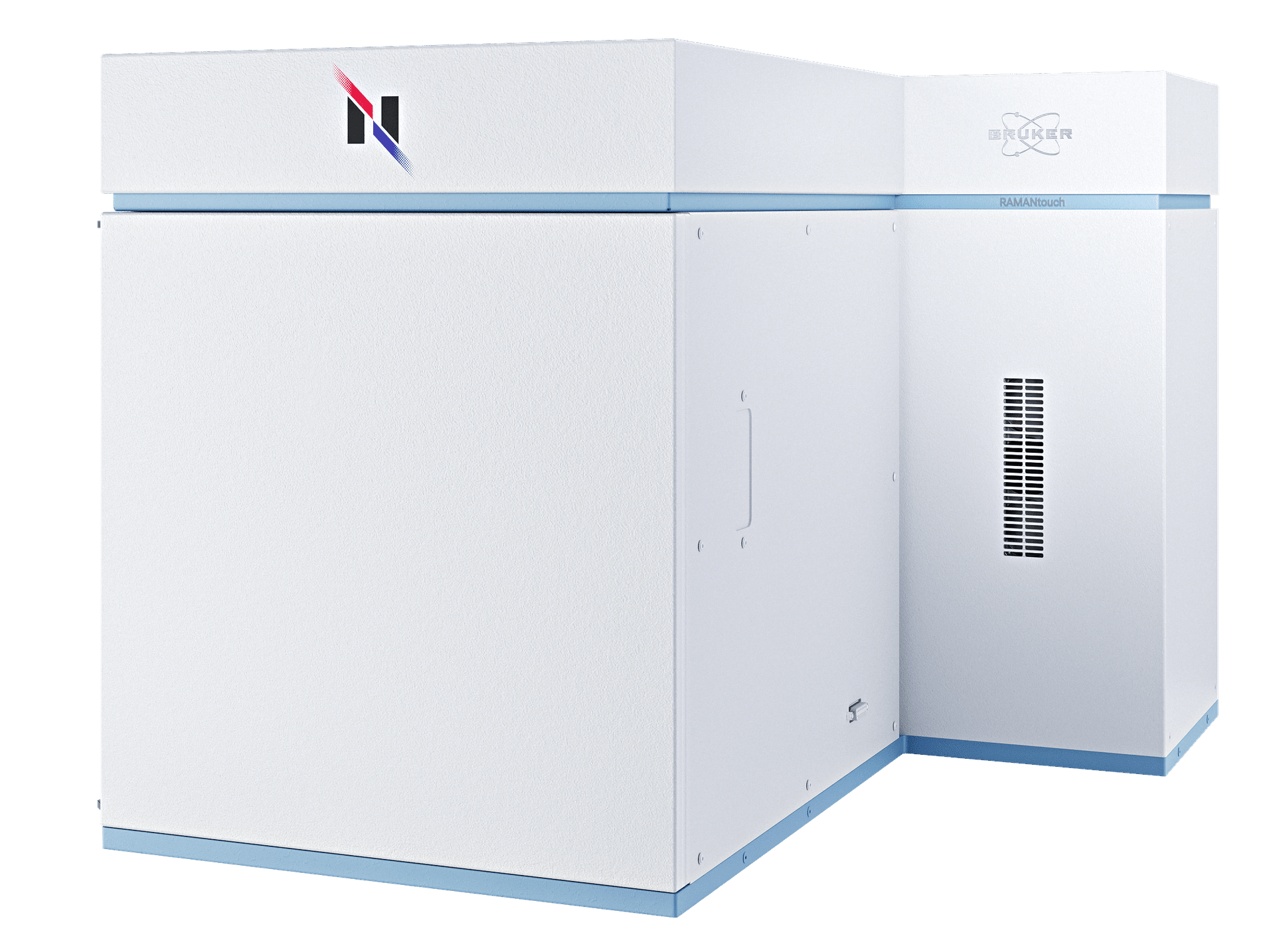
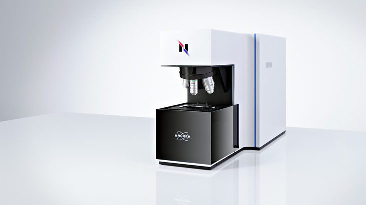
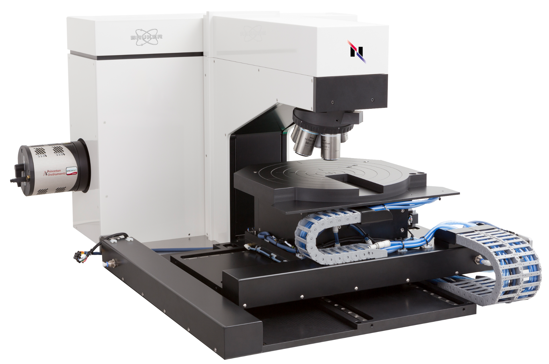
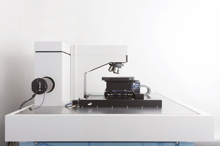
The Nanophoton RAMANdrive is designed to save time and improve the efficiency. Simply upload your data from your regular inspection tool and RAMANdrive identifies your areas of interest and moves the wafer automatically to the requested positions for a detailed analysis.
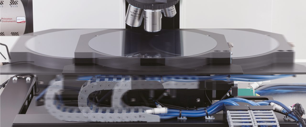
Key Features of the 300 mm Wafer Stage:
- Compatibility with Large Wafers: Supports wafers up to 300 mm, securely held in place by vacuum lines connected to small channels.
- Full Wafer Accessibility: Allows the laser to access the entire wafer surface.
- Tall Sample Accommodation: A deep channel in the stage permits analysis of taller samples.
Accurate and stable 300 mm wafer stage: For analysis, simply upload your data from your regular inspection tool and RAMANdrive identifies your areas of interest and moves the wafer automatically to the requested positions for a detailed analysis.
High-performance Raman imaging: Nanophoton’s advanced laser line illumination technology enables rapid data acquisition, capturing 400 spectra in a single laser shot. The system maintains peak speed without compromising spatial and spectral resolution, which is essential for detecting particles smaller than 100 nm and for stress or polytype analysis.
AreaFlash™ for complete laser coverage in Raman imaging: The AreaFlash technique enlarges the laser spot, ensuring that the excitation effectively covers the entire measurement region, thus delivering a complete and representative Raman image.
Determining the SiC polytype distribution: Here, the AreaFlash preview function quickly highlights variations in crystal structure.
Applications
- Raman Analysis of Particles Under 100 nm: With RAMANdrive’s high spatial resolution and high-quality dark-field microscopy, particles under 100 nm are readily identified.
- Visualizing Stress Distribution: In a SiC wafer, for example, cross-sectional Raman imaging effectively demonstrates stress distribution and highlights stress reduction achieved through polishing.
- Photoluminescence (PL) Imaging: PL imaging, using a 325 nm UV laser, reveals distributions of defects, impurities, and GaN itself.
Additional information